We all crave technology that is compact and cost-effective. Well, a few genius minds have got your point and created such technology. Say hello to NAND flash! NAND flash is a memory storage technology that is stable and doesn’t require power to preserve data. The purpose of this technology is to minimize the cost of storage capacity, which you can compare with your HDD or SSD.
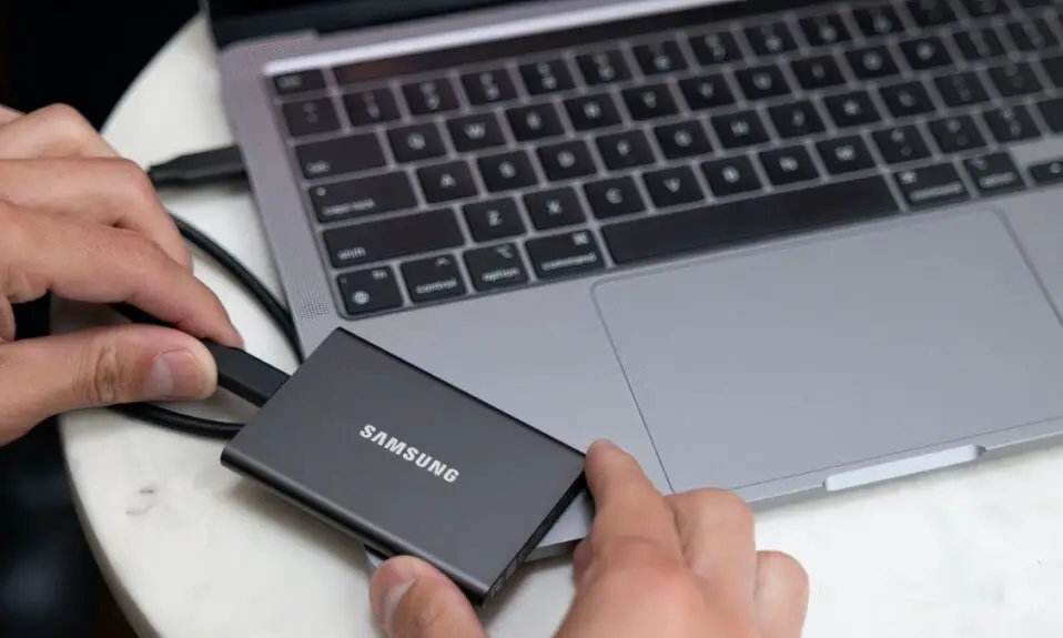
NAND flash has already created a standalone market for itself, where you can transfer a large volume of data. So, remember, small and compact gadgets that you use, like MP3 players, digital cameras, and USB flash drives, have adopted NAND flash technology.
How Does NAND Flash Technology Work?
Let us discuss the complicated working procedure of NAND flash technology in simple layman’s terms. Generally, flash memory storage uses a kind of erasable program, which is “read-only.” Meaning you can only see the contents but can’t edit them or delete them.
Now, in the case of a NAND flash storage drive, all the data is stored in a transistor – The Floating Gate. This particular transistor eventually powers up the storage device. Apart from that, there is another transistor, the Control Gate, which controls the amount of voltage.
The NAND technology, however, has a significant drawback. You can only use NAND-enabled storage devices for a limited time. After some time, it will wear off, meaning you can copy and delete files for a limited time; after that, the storage drive loses its capacity.
Pros and Cons of NAND?
The most significant reason why you can choose NAND flash storage is the fact it is cost-effective. Its per-byte cost is incomparable in the market.
A NAND-enabled storage chip is capable of high storage capacity. You may wonder how a small NAND chip can store a large volume of data.
Apart from that, a NAND-enabled storage chip lasts between 1,000 to 100,000 times of erasing data. However, it depends on its brand, model, and design.
Another significant factor is the fact that NAND chips are replaceable. You can easily replace the NAND-enabled chip with a new one once it wears off.
The availability of a NAND-powered chip is a problem. Because the technology is cost-effective, and as it is ideal for portable devices, you may need to search for it every time.
Conclusion
NAND flash technology is indeed a ground-breaking discovery. Yes, it has some problems where you can’t use it for eternity, but its per-byte cost-effectiveness is worth using it. NAND storage is ideal for tablets, USB drives, and digital cameras. The fact that you can store large files temporarily and erase them as per requirement makes data transfers so much easier.
We use NAND flash technology quite frequently. It has evolved the way we transfer files. You don’t need to depend on a CD-ROM to burn a disk; use a NAND storage chip instead.